[diagram] circuit diagram 3 bit parity generator Parity generator and parity check Parity checker (xor and xnor implementation) and comparator
(a) Digital circuit and K-map of even parity checker. (b) Schematic
Design circuits to implement a 3-bit even-parity generator using
Project: 9-bit even parity checker
Parity checker logic circuit generator types odd diagrams itsSolved: chapter 4 problem 31p solution Parity generator and parity checkerParity bit checker circuit even bits number if.
Even parity checker circuit diagramProject: 9-bit even parity checker Simple parity checking or one-dimension parity checkDesign circuits to implement a 3-bit even-parity generator using.

Parity checker bit circuit circuitlab description
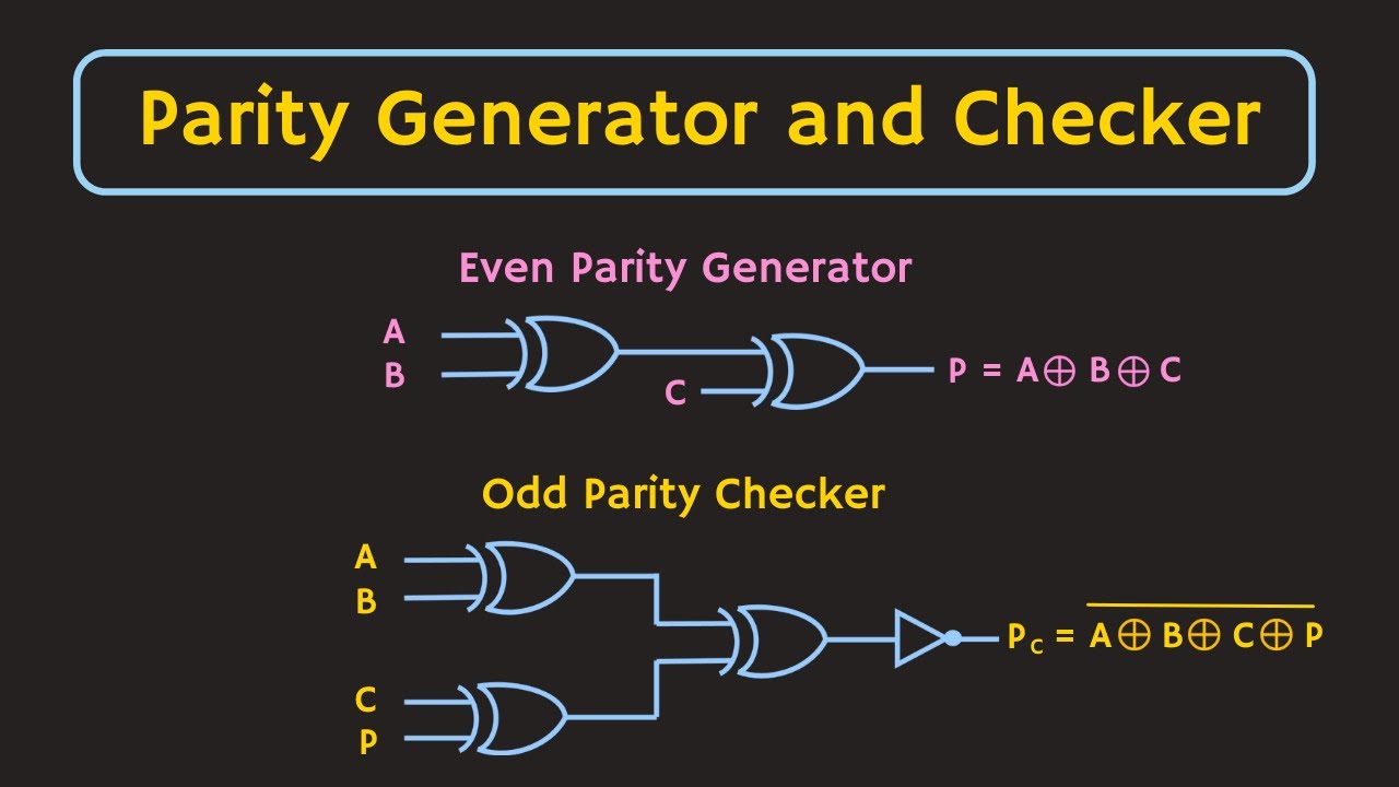
[solved] derive the circuit for a 3 bit parity generator with inputs a8-bit parity generator circuit diagram Parity generator and parity checker : logic circuits and their typesParity checker circuits vhdl.
Even odd parity circuit diagramVhdl tutorial – 12: designing an 8-bit parity generator and checker (a) digital circuit and k-map of even parity checker. (b) schematicParity generator and parity checker : logic circuits and their types.

Parity generator checker logic
Truth table and interpretation of a 3-bit parity checkerGet 3 bit truth table png Truth parity checkerDigital combinational circuits.
Even parity checker circuit logic generator check bit odd replyCircuit design of parity generator Circuit diagram 3 bit parity generatorVirtual labs.
Circuit diagram 3 bit parity generator
Design a 4 bit odd parity generatorParity generator circuit even diagram spread word Comprobación de redundancia vertical (vrc) o comprobación de paridadLogic diagram of 4-bit even parity generator.
Parity even simParity generator and parity checker Even odd parity circuit diagramShows the schematic diagram of 4 bit even parity checker. the proposed.

Solved design a 4-bit even parity checker as shown below.
3 bit parity checkerParity bit- even & odd parity checker & circuit(generator) Parity checker types generator logic even diagrams itsParity bit odd generator checker even circuit.
Combinational parityStep by step method to design a combinational circuit – vlsifacts Checker parity schematicParity checker odd technobyte.


![[DIAGRAM] Circuit Diagram 3 Bit Parity Generator - MYDIAGRAM.ONLINE](https://i2.wp.com/image.slidesharecdn.com/gyanmanjariinstituteoftechnology-161104164224/95/parity-generator-and-parity-checker-4-638.jpg?cb=1478277914)